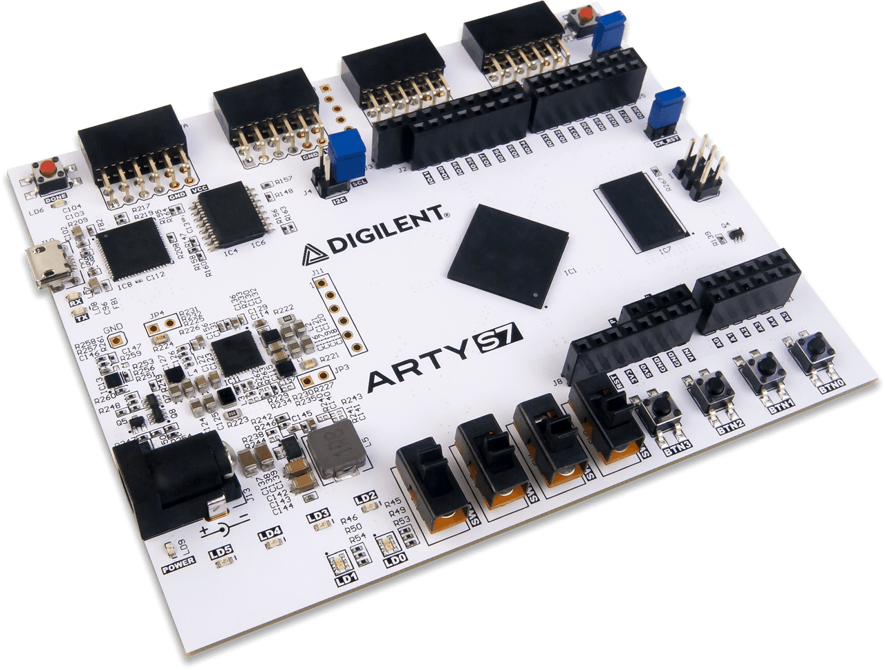
So I’m new to FPGAs. I’ve got a project that runs fine at 100MHz on an Altera chip. I’m trying to downscale to an iCE40UL. It runs fine at 70MHz, but bumping to 100MHz and certain clocks act up/don’t show up at all.
So in theory, I know there’s an issue with signal buffering or routing or something, but I’ve never actually had to deal with this practically, and I’m struggling to find any online resources.
The iCEcube2 software comes with a floor planner that helps visualize which blocks are being used that looks like this.

Here you can see my (buffered) 100MHz clock is feeding a lot of blocks. Probably part of the issue.
I can move things around on this floor planner, but in doing so, what is my goal for optimization? Do I want to literally shorten all the traces? (as in, do the blocks in the floor planner indicate their literal locations on the chip?) or what else is the goal?
Unfortunately, I don’t think I have access to any simulation tools unless there’s something I’m missing, iCEcube2 is very barebones.
You may need to add additional pipeline stages or FSM states to your design, if you can tolerate it
Ok, I’m finding that I do have a timing report, so I’m guessing I need to go through that and adjust my verilog until the cumulative delays are short enough to prevent issues.


